


")
")
B.Tech. Electronics Engineering (VLSI Design and Technology)
The B.Tech. Electronics and Communications Engineering programme at GITAM School of Technology, Hyderabad, is designed to foster innovation in the electronics and telecom sectors. The curriculum is guided by academic leaders from premier institutions such as IITs and NITs, and developed in collaboration with top multinational corporations.
The programme aims to equip students with a strong foundation in both theoretical concepts and practical applications, ensuring they are ready to drive technological advancements and contribute to societal benefits as entrepreneurial innovators.
Eligibility
A minimum of 50% or 5.0 CGPA aggregate marks in Intermediate or 10+2 examination from a recognized central / state board with Physics, Chemistry & Mathematics subjects.
Students scoring between 50–60% must meet at least one of the following criteria to be eligible:
a. Score over 42% (85/200) in GAT and over 75% in X Standard.
b. Score over 55% (110/200) in GAT.
c. Score over 85% in X Standard.
Additionally, such students must sign a waiver form if companies require more than 60% in Intermediate or 12th grade for placements.
Scope of the Programme
This programme offers strong career opportunities in semiconductor design, microelectronics and FPGA prototype development. The demand for VLSI professionals is growing rapidly due to advancements in AI, 5G, and IoT, leading to job roles in industries such as chip manufacturing, telecommunication, and consumer electronics. Graduates can pursue roles like VLSI design engineer, physical design engineer, and verification engineer, contributing to cutting-edge technological innovations. Additionally, the field provides opportunities for higher studies and research in next-generation novel electronic devices and circuits.
Outcomes and Objectives
PO1 - Engineering knowledge: Apply the knowledge of mathematics, science, engineering fundamentals, and an engineering specialization to the solution of complex engineering problems.
PO2 - Problem analysis: Identify, formulate, research literature, and analyze complex engineering problems reaching substantiated conclusions using first principles of mathematics, natural sciences, and engineering sciences.
PO3 - Design/development of solutions: Design solutions for complex engineering problems and design system components or processes that meet the specified needs with appropriate consideration for the public health and safety, and the cultural, societal, and environmental considerations.
PO4 - Conduct investigations of complex problems: Use research-based knowledge and research methods including design of experiments, analysis and interpretation of data, and synthesis of the information to provide valid conclusions.
PO5 - Modern tool usage: Create, select, and apply appropriate techniques, resources, and modern engineering and IT tools including prediction and modelling to complex engineering activities with an understanding of the limitations
PO6 - The engineer and society: Apply reasoning informed by the contextual knowledge to assess societal, health, safety, legal and cultural issues and the consequent responsibilities relevant to the professional engineering practice.
PO7 - Environment and sustainability: Understand the impact of the professional engineering solutions in societal and environmental contexts, and demonstrate the knowledge of, and need for sustainable development.
PO8 - Ethics: Apply ethical principles and commit to professional ethics and responsibilities and norms of the engineering practice.
PO9 - Individual and teamwork: Function effectively as an individual, and as a member or leader in diverse teams, and in multidisciplinary settings
PO10 - Communication: Communicate effectively on complex engineering activities with the engineering community and with society at large, such as, being able to comprehend and write effective reports and design documentation, make effective presentations, and give and receive clear instructions.
PO11 - Project management and finance: Demonstrate knowledge and understanding of the engineering and management principles and apply these to one’s own work, as a member and leader in a team, to manage projects and in multidisciplinary environments.
PO12 - Life-long learning: Recognize the need for and have the preparation and ability to engage in independent and life-long learning in the broadest context of technological change.
PEO 1: Demonstrate comprehensive knowledge of analytical foundations to Electronics and Communication Engineering in terms of founding principles of circuits, design, computing, signal processing and communication.
PEO 2: Demonstrate critical thinking and problem-solving abilities to handle the real-world problems by applying theoretical foundations and practical skills in different fields of Electronics and Communication Engineering.
PEO 3: Exhibit qualities of teamwork, appreciation of collaboration that entails inter-disciplinary endeavors and the potential impact of technology on society.
PEO 4: Develop creativity, Research related skills, self-learning, entrepreneurial and leadership skills in order to meet the ever-changing needs and challenges in the profession.
PSO 1: Design and research analog, digital, and mixed-signal integrated circuits using different VLSI design methodologies involving industry-standard tools, balancing tradeoffs in area, power, speed, and reliability.
PSO 2: Apply research methods to formulate and solve research problems in integrated circuit design of contemporary societal relevance.
PSO 3: Survey and present state-of-the-art circuit/system design procedures for VLSI Design and Fabrication.
Key Highlights
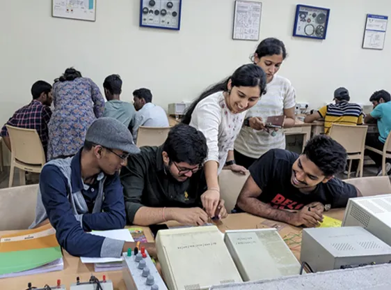
Centers of Excellence & Infrastructure
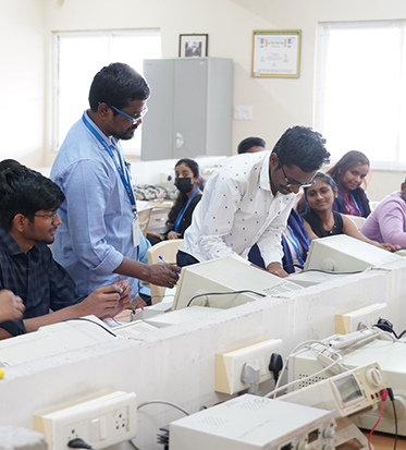
The programme offers access to the VLSI Physical Design Lab, Digital Design and Verification Lab, Analog & Mixed Signal Design Lab, and RTL Design and Synthesis Lab.
Research Centre
Engage in multidisciplinary research focusing on VLSI design and semiconductor technologies.
Industry & Academic Collaborations
Earn 24 credits from various schools such as Business, Humanities, Law, Architecture, and Sciences.
Venture Development Centre
A mandatory 2-credit course fostering hands-on learning and innovation.
Technology Exploration and Product Engineering
A mandatory 2-credit foundational course focusing on problem-solving, design thinking, collaboration, ethical considerations, and sustainability. Students engage in a Problem-Based Learning approach to tackle real-world challenges.
Syllabus
The curriculum includes:
- VLSI design
- Digital System Design
- Analog IC design
- Low power VLSI design
- Algorithms for VLSI design
- VLSI signal processing
- Design for Testability
Career Options
India's Electronics and Communications Engineering (ECE) sector is a cornerstone of the digital world, driving advancements in industries like IoT, robotics, healthcare, and more. With the electronics market in India expected to reach $400 billion, driven by a 41% CAGR, ECE graduates are well-positioned for diverse and in-demand career paths in both technological and manufacturing sectors.
- IC Design Engineer
- Physical Design Engineer
- Test Engineer
- ASIC Design Engineer
- Applications Engineer
- FPGA Design Engineer
- SoC Developer
- Verification Engineer
- Product Engineer
- Technical Manager
- Process Integration Engineer
Star Recruiters


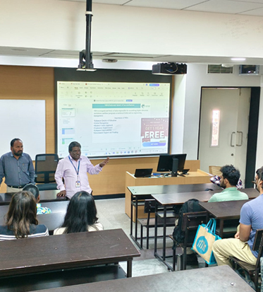
School Leadership


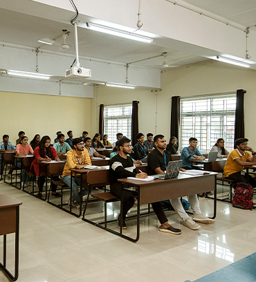
Multidisciplinary and Interdisciplinary Applied Education


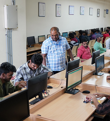
Infrastructure and Facilities


Fee Structure
B.Tech. Electronics Engineering (VLSI Design and Technology)
1st Year
₹ 2,83,500
2nd Year
₹ 2,97,600
3rd Year
₹ 3,12,400
4th Year
₹ 3,28,000
Scholarships
Merit-Based Scholarships
The scholarship from GAT/National/State Entrance Tests applies only in the first year. To continue receiving it in subsequent years, a minimum CGPA of 8.0 must be maintained.
Apart from the above, the following scholarships are also offered to eligible students.
- Employee Children Scholarships: (60%, 40%, and 20%)
- Loyalty Scholarships: (10% for Any alumni returning to do higher studies/Children of Alumni/Real siblings (Not applicable to step siblings or cousins)/Children of retired employees of GITAM/Spouse of GITAM employees).
- Sports Scholarships: (100%, 75%, 50%, 25% and 15%)
Need-Based Scholarships
- To be eligible for the need-based scholarship, the combined income of both parents/guardians of the eligible student/If the student is married, the combined income of the family, i.e., the student's and spouse's income, must be less than 12.00 LPA.
- The candidates admitted through merit scholarship in the slabs of 75%, 60%, 40%, 25%,and 15%, and the parents/guardians combined income is less than the prescribed limits are eligible for the additional need-based scholarship.
| Scholarship % | Upgraded Scholarship % |
|---|---|
| 75% | 100% |
| 60% | 75% |
| 40% | 60% |
| 25% | 40% |
| 15% | 25% |
Scholarships For Accommodation
- In addition, students awarded need-based scholarships after merit scholarships will receive an additional 20% scholarship specifically allocated for hostel fees at GITAM for slabs: 15%, 25%, 40%, and 60%.
- Students awarded 75% & 100% scholarships are also awarded the same percentage in the hostel and food fees.
| Year | Scholarship % | GAT 2025 Score | JEE(Main) 2025 | AP / TS EAPCET | SAT 2025 | NID DAT 2025 |
|---|---|---|---|---|---|---|
| 2025-26 | 100 | 141 - 200 | >=97.00 | 1 – 100 | 1501-1600 | >=97 |
| 75 | 131 - 140 | 94-96.99 | 101 - 250 | 1451 - 1500 | 94 - 96 | |
| 60 | 121 - 130 | 92 - 93.99 | 251 - 1000 | 1401 - 1450 | 92 - 93 | |
| 40 | 111 - 120 | 90 - 91.99 | 1001 - 2500 | 1351 - 1400 | 90 - 91 | |
| 25 | 101 - 110 | 88 - 89.99 | 2501 - 5000 | 1301 - 1350 | 87 - 89 | |
| 15 | 86 - 100 | 85 - 87.99 | 5001 - 25000 | 1200 - 1300 | 84 - 86 |
Note: Terms & Conditions Applied
Lateral Entry
| Year | Scholarship % | GAT 2025 Score | AP/TS ECET & DCET 2025 Branch Rank | State Technical Board % Except (AP,TS & KA) |
|---|---|---|---|---|
| 2025-26 | 100 | 141 - 200 | 1 – 100 | 95 - 100 |
| 75 | 131 - 140 | 101 - 500 | 91 - 94.99 | |
| 60 | 121 - 130 | 501 - 1000 | 88 - 90.99 | |
| 40 | 111 - 120 | 1001 - 1500 | 83- 87.99 | |
| 25 | 101 - 110 | 1501 - 3000 | 80 - 82.99 | |
| 15 | 86 - 100 | 3001 - 5000 | 70 - 79.99 |
Note: Terms & Conditions Applied
